At present, the progress of RFID tag technology mainly focuses on the manufacturing materials and printing processes of antennas and chips, and has become an important research direction of printed electronics technology.
Compared with other technologies for RFID tag production, the birth of printing technology makes RFID tags have unparalleled advantages in low cost, high efficiency and environmental protection, which provides great possibilities for their further role in the civil field.
Progress in manufacturing materials
1. Antenna material
The mainstream RFID antennas are mainly made of copper and aluminum, and are manufactured by coil winding and etching processes respectively. The products have great advantages in reliability and service life, so they occupy most of the market.
However, with the rise of nanotechnology, nano inks (made of conductive materials) that can directly print RFID antennas pose challenges to existing materials. According to statistics from IDtechEX (a well-known market research company), the global conductive ink market accounted for US $ 2.86 billion in 2012. It is expected that the conductive ink market will reach US $ 3.36 billion in 2018. At that time, the market for nano silver conductive ink and nano copper conductive ink will reach 735 million US dollars.
However, the nano-conductive ink printing RFID antenna technology still faces the problems of ink adhesion, friction resistance, printing uniformity, conductivity and oxidation resistance.
(1) Nano silver conductive ink
Nano silver conductive ink has excellent conductivity, anti-oxidation, coupled with its high technology maturity, it is the first choice material for printing RFID antenna.
The relevant research group of Huazhong University of Science and Technology used sodium hypophosphite as the reducing agent, sodium hexametaphosphate as the dispersant, and PVP as the protective agent, and reacted with the silver nitrate solution to prepare a fuchsia silver sol, adding a pH adjuster to adjust the pH of the silver sol Adjust to 3, after filtering, passivation, washing and other operations, vacuum drying at 60 ℃ temperature environment to obtain nano-silver powder with an average particle size of about 30nm, then add it to FA-406 ink to configure a conductive ink, after curing, the Conductive ink has good flexibility and heat and humidity resistance, and has high conductivity and good printing uniformity.
(2) Nano copper conductive ink
Although the conductivity of nano-copper conductive ink is slightly worse than that of nano-silver conductive ink, the price has a great competitive advantage, and it has become a research hotspot in recent years. However, the chemical nature of copper is active, which makes it difficult to avoid the oxidation of nano-copper particles in synthesis and application.
A company has successfully prepared spherical nanocopper with a diameter of 30-50 nm by using the reduction method in the organic solvent ethylene glycol, and there are no other oxides. This shows that ethylene glycol can prevent the nano copper from oxidizing, and at the same time, polyethylene glycol The dispersant can increase the dispersion stability and uniformity of the nano copper particles.
2. Chip material
In the field of chip manufacturing, the benchmark for measuring the manufacturing process is the width of the connection between the transistor and the wire in the chip, that is, the line width. The thinner the width, the more accurate the manufacturing process. Limited by the size of atomic components, the line width of semiconductor chips has its physical limit, and the chip size cannot be infinitely small. Therefore, it is difficult to increase the frequency of power on and off to a certain extent.
Using carbon nanotubes (CNTs) to replace silicon transistors is the best way to break this bottleneck. Compared with other semiconductor materials, CNTs are not only small in size, excellent in electrical performance, stable in physical and chemical properties, but also have the advantages of less heat generation and higher operating frequency of transistors constructed by CNTs. At the same time, CNTs are easy to achieve solution, separation and purification After the CNTs ink can print high-performance thin-film transistor devices.
Inevitably, CNTs also have the disadvantage that the prepared CNTs contain both metallic and semiconducting CNTs. Therefore, in the field of chip manufacturing, it needs to be separated to obtain semiconductor CNTs to play a corresponding role.
At present, the separation of single-walled CNTs is generally based on chemical methods, which are relatively mature, including electrophoretic separation and chromatographic method, but often involve a variety of chemical reagents, such as the addition of surfactants will cause doping Miscellaneous effects, so separation requires multiple physical and chemical processes to complete.
In recent years, a new method of separating CNTs has emerged-the Coulomb explosion method. The Coulomb explosion method uses the principle of electrostatic repulsion to bring a bundle of single-walled CNTs with the same kind of charge. When the repulsive force between the charges is greater than the van der Waals force between the CNTs, a Coulomb explosion occurs. This explosion can separate a bundle of carbon nanotubes from each other, forming a unique and novel radial pattern, named "nanotree". Tests such as Raman spectra proved that the separated CNTs have a small diameter, less than 3nm, and even single CNTs with complete structure appear.
At the same time, there are other new technologies, such as the use of different sequences of DNA to identify metallic and semiconductor single-walled CNTs. Although DNA recognition is sensitive, it is costly and time-consuming. To shorten this duration, two-phase extraction can be used to separate single-walled CNTs with different properties. The entire process takes only 4 minutes, which is tens of times faster than traditional methods, and the cost is greatly reduced. The real application provides the possibility.
Square Double Sided Light Box
Square Double Sided Light Box
Specifications:
|
Material
|
Aluminium/ Stainless steel/ Acrylic Panel
|
|
Size
|
Customized
|
|
Lighting Colour
|
White/ Pink/ Red/ Green/ Blue/ Yellow etc.
|
|
Lighting Source
|
Led Strips/LED module
|
|
Features
|
Waterproof/ Low Consumption / Bold Visual Effect etc.
|
|
Safe Voltage
|
Normally 12 DC, 110V~230V
|
|
Processing
|
Cutting, Sanding, Bending, Glue, Wiring, etc.
|
|
Application
|
Both indoor/ outdoor Decoration and advertisement.
|
|
Average Life Time
|
>60,000 hours
|
|
Working temperature
|
-20℃~60℃
|
|
Installtion Method
|
3M adhesive, Back screw bolts fixing or hanging, with 1:1 fixing template and accessories for Installation Reference
|
|
Packaging
|
Covered with bubble wrap and foam inside,and packed with wooden case outside. Also can be packed as your requirements.
|
|
Shipment
|
By express:(TNT/UPS/DHL etc.):4-5 Days
|
|
|
By Air:5-7 Days
|
|
|
By Ship:25-35 Days
|
|
OEM/ODM
|
Accepted
|
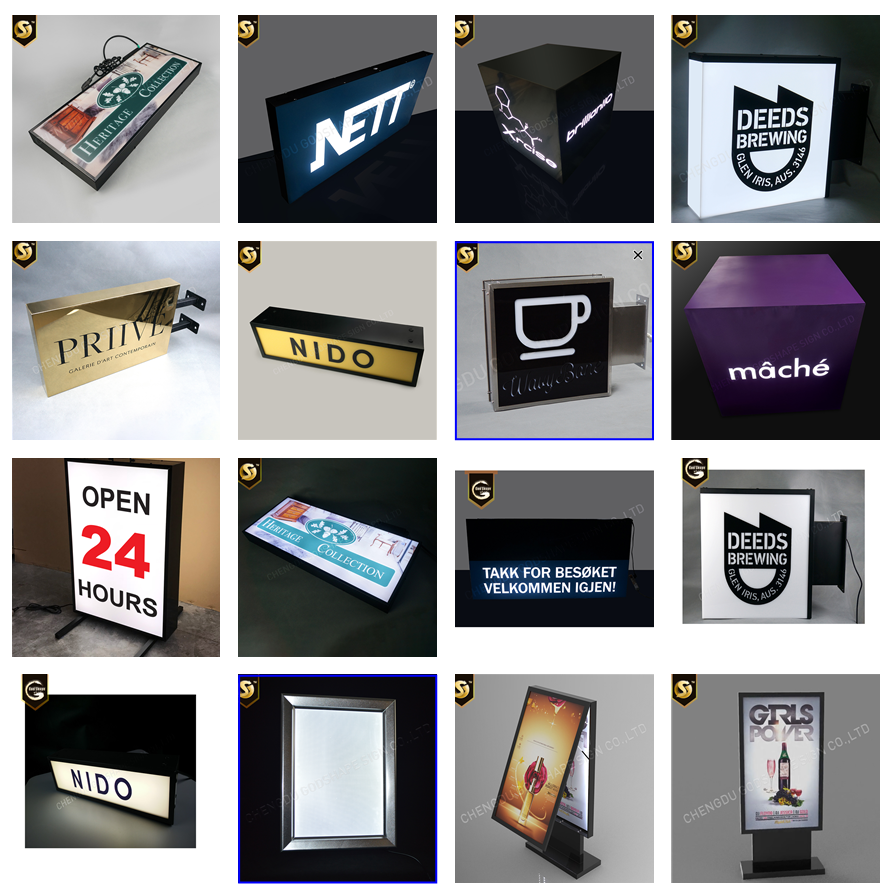
Models pictures:

FAQ
Q: Are you a trading company or factory?
A: We are factory.
Q: What is the MOQ?
A: No MOQ required normally, that means you can always ask for a sample first. But remember the sample freight is at your own cost.
Q: Do I have to have a design to inquire?
A: Yes! A well made design/artwork is the most helpful thing to get an exact quote. However, if you really do not have a design...just let us know your idea, we'll cover it.
Lightboxes Signage,Double Sided Light Box,Double Sided Light Box Sign,Square Double Sided Light Box
Chengdu GodShape Sign Co., Ltd , https://www.signsgs.com
